 |
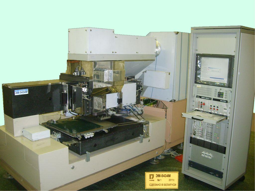
EМ-5434M HIGH DENSITY INTEGRATION PCB STEPPER
EM-5434M stepper is designed to enable a lithography process in the production of PCBs (IC Substrate) for flip-chip packaging (BGA/CSP).
The universality of the tool lies in capability to work with thick photoresist (50µm) and to control the resist side wall angle.
Part number:
Supplier:
KBTEM-OMO JSCDescription
Specifications
Lens resolution L/S, µm 8
Lens working field, mm 70x250; 85x228
Projection imaging scale 1:1
Automatic scale correction range, ppm ±1000
Lens distortion, no more than, µm ±2.5
Depth of focus, µm ±100
Working wavelengths i-(365nm)
h-(405nm)
g-(436nm)
Exposure light power density in the PCB panel plane, mW/cm2 220
Irradiation uniformity in the image plane, not less than, % ±5
Exposure dose error, % ±3
Reticle size, mm 254х305
Max substrate size, mm 610x610
Power consumption, not more than, kW 7