 |
EМ-5534 BUMPING STEPPER
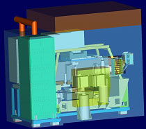
EМ-5534 stepper aligns and enables the projection transfer of the reticle image in 1:1 ratio onto the photoresist coated wafer and the further step-and-repeat imaging over the entire wafer. EМ-5534 stepper is designed to enable the lithography process in thick (up to 200 μm) photoresist layers. It can be employed in semiconductor die solder and gold bumping processes, as well as in photolithography processes for MEMS.
Part number:
Supplier:
KBTEM-OMO JSCDescription
Wafer diameter, inch 6, 8, 12, 18
Reticle size, inch 6
Photolithography resolution(L/S):
- 1 µm resist thickness, µm 4
- 30 µm resist thickness, µm 5
Depth of focus, µm ±50
Lens working field, mm 115х120
Automatic scale correction range, ррm ±30
Working wavelength, nm 350-450 (i+h+g-line)
Power consumption, not more than, kW 6.5
Reticle size, inch 6
Photolithography resolution(L/S):
- 1 µm resist thickness, µm 4
- 30 µm resist thickness, µm 5
Depth of focus, µm ±50
Lens working field, mm 115х120
Automatic scale correction range, ррm ±30
Working wavelength, nm 350-450 (i+h+g-line)
Power consumption, not more than, kW 6.5